Senior Editor: Alan Agbele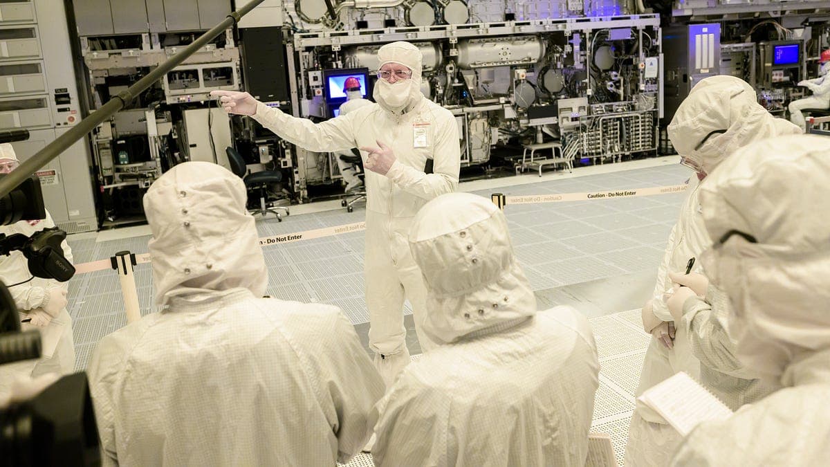
Intel has begun shipping the first commercial silicon produced using High-NA EUV lithography, a manufacturing milestone that positions the company to challenge its foundry rivals in the race for smaller, more powerful chips. The move signals Intel's determination to reclaim process leadership with technology that no other chipmaker has yet deployed in volume production.
The Technology Behind High-NA EUV
High-NA EUV stands for High Numerical Aperture Extreme Ultraviolet lithography. It uses a 0.55 numerical aperture lens, compared to 0.33 in the current EUV systems, to achieve finer pattern resolution. This allows chipmakers to print smaller transistors with higher density, enabling more powerful and energy-efficient chips.
The shift to High-NA EUV is not incremental. It requires entirely new optics, mirrors and vacuum chambers. ASML, the Dutch company that holds a monopoly on EUV lithography, delivered the first High-NA EUV system to Intel in late 2023. Intel has since integrated it into its 18A process node, which is expected to compete directly with TSMC's N2 and Samsung's SF2 technologies.
Why This Matters
Intel's early delivery of High-NA EUV silicon has immediate consequences for the semiconductor industry. For the first time in years, Intel has a tangible manufacturing advantage over TSMC and Samsung, both of which are still evaluating High-NA EUV for their own roadmaps. If Intel can maintain yield and ramp volume, it could win back major customers for its foundry business, including those designing AI accelerators and high-performance computing chips.
The broader implication is a potential shift in the balance of power in chip manufacturing. TSMC currently dominates with its N3 and N5 nodes, but Intel's 18A process, built with High-NA EUV, promises comparable or better density and performance. For consumers, this could mean faster, cooler-running processors in laptops, servers and smartphones within the next two years.
Intel's move also pressures ASML's supply chain. With only a handful of High-NA EUV systems produced each year, Intel's early commitment locks up tool availability, delaying rivals' access. This strategic advantage could compound as Intel refines its process while competitors play catch-up.
What Comes Next
Intel plans to scale High-NA EUV across its 18A production lines throughout 2025. The company has not disclosed which specific products will first use the new silicon, but analysts expect server-class Xeon processors and future AI accelerators to be among the initial beneficiaries. The technology will also underpin Intel's push into external foundry services, a key part of CEO Pat Gelsinger's turnaround strategy.
Rivals are not standing still. TSMC is expected to deploy High-NA EUV in its A16 node, slated for 2026, while Samsung is developing similar tools for its SF1.4 process. The race to master High-NA EUV will define the next decade of semiconductor advancement, and Intel has fired the first shot.