Editor: Porcia Akua Holmes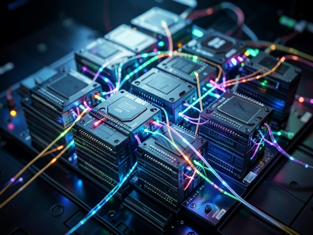
The AI industry faces a fundamental problem: how to connect thousands of GPUs without choking performance. Inside the race to scale AI hardware, optical links are moving from the data center edge to the very heart of the processor package. As hyperscale data centers push beyond the limits of copper cabling, a new class of photonic interconnects is emerging as the critical piece of infrastructure.
The Optical Imperative
Moore's Law has slowed to a crawl, forcing AI architects to stitch dozens of accelerators into single logical machines. But the fabric that binds them, copper cabling, has hit a physical wall. Nick Harris, chief executive of photonics firm Lightmatter, told Tom's Hardware Premium that copper cable length is roughly two meters, and the industry has already reached that limit. “Moore's Law is deader than a doornail, absolutely just toast,” he said. The implication is clear: the way to gain performance is no longer packing more silicon onto a die but networking hundreds of chips together with ultra-low latency and very high bandwidth.
The Scaling Hierarchy
Data centers rely on three tiers of interconnect. There is scale-up inside a single rack of up to 144 GPUs. There is scale-out linking racks into clusters. And there is scale-across connecting entire data centers. Each tier demands different levels of latency and bandwidth. Optical technology is now becoming essential at every level.
Harris expects near-package optics to be the test bed for the industry in 2027 and 2028. Lightmatter is already building co-packaged optics parts at TSMC and GlobalFoundries, with shipping planned for 2028. At the same time, the company is working with customers on the more integrated interposer approach, which Harris says is for those who realize they would like an advantage in the market.
The movement has drawn attention from major players. Earlier this month, Elon Musk received regulatory clearance to purchase Mesh Optical, a move that underscores how critical interconnects have become to AI infrastructure. Mesh Optical joins Musk's growing stack of technologies aimed at powering TeraFab and SpaceX's AI ambitions.
Why This Matters
The interconnect race will determine which companies can operate the largest AI training clusters. Hyperscalers that adopt optics early will enjoy lower latency and higher throughput, directly translating into faster model training and lower costs per inference. GPU vendors like Nvidia, which already integrates 72 to 144 GPUs per rack using proprietary switches, must now decide whether to embrace open optical standards or defend their existing copper-based architectures.
The energy math is also consequential. Polina Bayvel, professor of optical communications at University College London, notes that roughly 20 percent of a data center's energy is consumed by networking. Every watt saved through optics will be reinvested into additional GPUs rather than reducing the facility's carbon footprint. This means the environmental benefit of optical interconnects is largely indirect, enabling more compute per watt rather than cutting absolute energy use.
For AI startups and enterprises, the shift could widen the gap between those who can afford the most advanced optical infrastructure and those who cannot. As the cost of integrating photonics into chip packaging falls, the barrier to entry for frontier model training may shrink. But for now, the battle for scale remains tightly coupled with the battle over the fabric that connects the chips.