Editor: Porcia Akua Holmes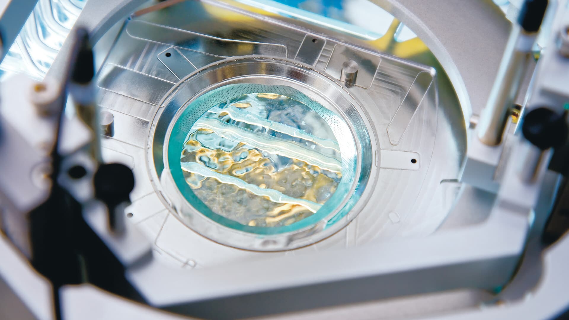
In 2003, the semiconductor industry faced a crisis. For decades, chipmakers had shrunk transistors by using ever-shorter wavelengths of light to etch patterns onto silicon. But the next step, moving from 193nm to 157nm lithography, proved too expensive and unreliable. Then an unexpected solution emerged: a thin layer of water.
The Lithography Bottleneck
Conventional dry lithography operates with air between the final lens and the silicon wafer. The refractive index of air limits the numerical aperture, the key metric for resolution, to about 0.93. Chipmakers had reached that ceiling with 193nm light sources. Shifting to 157nm would have required entirely new optics and reticle materials, driving costs past what the industry could sustain.
Immersion lithography solved this by replacing air with deionized water, which has a refractive index of 1.44. This change boosted the effective numerical aperture above 1.0, enabling features as small as 40nm without changing the light source. The idea had been explored in laboratories for years, but mass production reliability remained uncertain.
Three factors made immersion feasible for high-volume manufacturing:
Industry Adoption and Legacy
ASML delivered the first production immersion scanners in 2004. TSMC and Intel quickly adopted the technology for critical layers. Within two years, most leading-edge chips were being manufactured using immersion lithography. The technique delivered the resolution needed for the 65nm, 45nm and 32nm nodes, keeping Moore's Law alive.
The industry spent billions developing extreme ultraviolet lithography as the eventual successor. But EUV faced its own delays, and immersion filled the gap. Many chipmakers continued using immersion for less critical layers even after EUV entered production around 2018. The combination of 193nm light and water remains in use today for memory and analog components.
Why This Matters
Without immersion lithography, Moore's Law likely would have ended around 2005. The pause would have delayed the performance gains that powered the smartphone era, cloud computing and modern artificial intelligence. Immersion gave researchers time to solve the immense challenges of EUV, ensuring that transistor scaling could continue for another decade.
This technology also reshaped the economics of chip fabrication. The tools required sophisticated water handling and thermal management, raising equipment costs. But the alternative, developing entirely new 157nm infrastructure, would have been far more expensive. Immersion allowed chipmakers to amortize their existing investments in 193nm lasers and lenses while extending their capabilities.
For consumers, the impact is invisible but fundamental. Every processor designed after 2005 relies on patterns created with immersion lithography. The efficiency gains from smaller transistors reduced power consumption in laptops, phones and data centers. Without this innovation, the trajectory of the entire tech industry would look dramatically different.