Senior Editor: Alan Agbele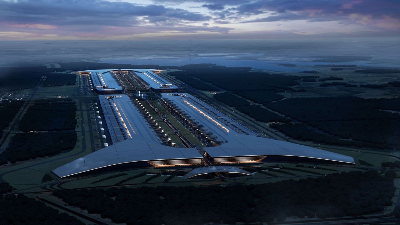
SpaceX and Tesla have officially unveiled the first phase of their Terafab project, a semiconductor manufacturing campus in Grimes County, Texas, that will dwarf existing facilities. The initial investment of $16.8 billion and a planned 100 million square feet of manufacturing space signal a bold bet on vertical integration for chip production.
Scale Beyond Existing Fabs
The 100 million square feet of manufacturing space at Terafab exceeds the total area of Samsung’s massive Pyeongtaek campus, which spans about 31.1 million square feet. However, that figure does not refer to cleanroom space alone; it includes supporting areas such as logistics and administration. Even so, the project represents a step change in the size of semiconductor facilities.
Vertical Integration as a Strategy
Unlike traditional semiconductor fabs, Terafab will house logic production, memory fabrication, packaging and testing in one complex. This consolidation aims to shorten production cycles and improve time-to-yield by enabling faster iterative improvements. The approach mirrors Tesla’s vertical integration in vehicle manufacturing but applied to chips.
Elon Musk’s companies, including Tesla, SpaceX and xAI, already consume a large share of available contract chipmaking services. The Terafab project could reduce that reliance and give Musk’s ventures more control over their supply chain. The facility is expected to use water from Gibbons Creek Reservoir and include on-site wastewater treatment and recycling.
Why This Matters
Terafab could reshape the semiconductor industry by proving that a single company can economically build and operate a massive, vertically integrated fab. If successful, it may encourage other large tech firms to pursue similar strategies, increasing competition for traditional foundries like TSMC and Samsung. The project also underscores the strategic importance of domestic chip manufacturing for AI and autonomous systems, with implications for national security and economic competitiveness.
Furthermore, the scale of Terafab raises questions about the future of the semiconductor workforce. The promise of 3,000 jobs in a rural Texas county highlights the potential for high-tech employment to spread beyond traditional tech hubs. However, the success of the project will depend on whether the demand for chips from Musk’s companies reaches the projected 1 terawatt of compute per year.