Editor: Porcia Akua Holmes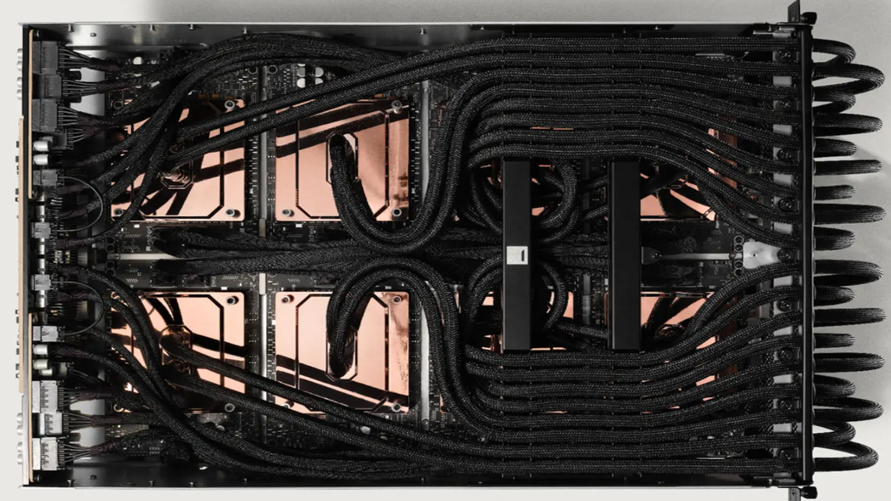
Etched, a startup designing processors exclusively for AI inference, has closed $300 million in new funding from SK Hynix and other investors, pushing its valuation to $10.3 billion. The company argues that conventional GPUs waste power on inference workloads and that its custom architecture can deliver higher throughput with lower energy consumption.
Inference-First Design Breaks From GPU Model
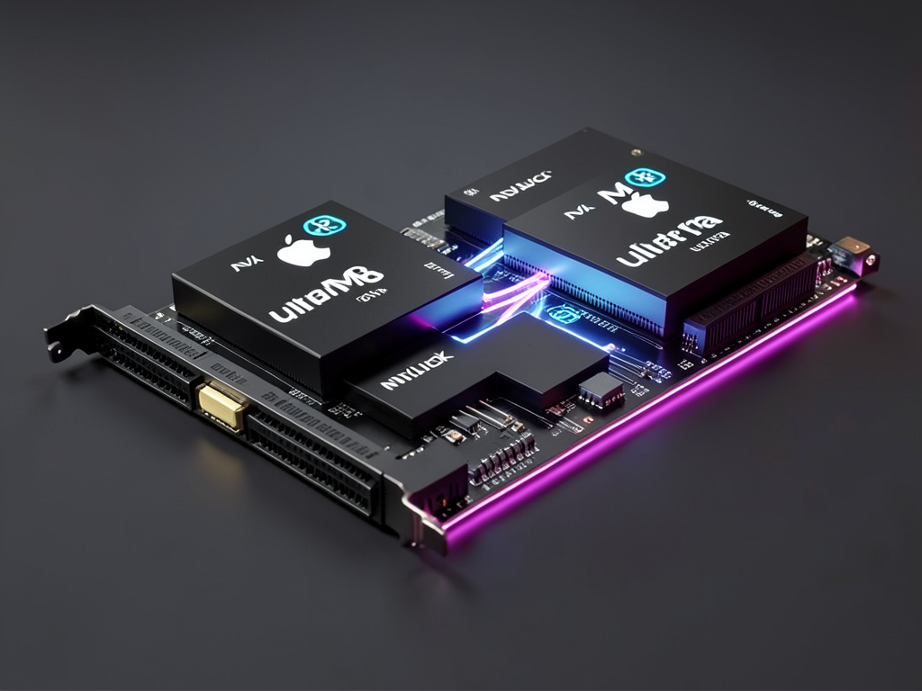
Most AI chips today are built for training large models and repurposed for inference. Etched takes the opposite approach. Its processors use Low Voltage Inference (LVI) technology to run math blocks at under half the voltage of typical AI chips. This allows the chip to pack multiple times the FLOPs density without thermal throttling, a problem that limits performance in conventional GPUs.
The company also developed Cluster Scale Memory (CSM), a shared memory pool that combines HBM and SRAM. This reduces latency because processors do not need to move data through multiple memory layers during inference tasks. Co-founder Robert Wachen described the system as solving both memory capacity and memory-to-memory latency issues simultaneously.
Etched claims that many AI models spend substantial time shuttling data between chips, memory and networking hardware. The CSM architecture cuts those delays by minimizing additional memory layers during transfers.
Why This Matters
The AI industry is shifting focus from training ever-larger models to deploying them efficiently at scale. Inference workloads already account for a growing share of AI compute costs, and general-purpose GPUs are not optimized for this stage. Etched's approach could lower the cost and energy required to run models in production, making AI services more accessible and sustainable.
For companies like SK Hynix, backing Etched provides a foothold in the fast-growing inference chip market and a channel for its memory products. The partnership also signals that memory suppliers see value in specialized architectures that maximize the performance of their HBM and SRAM technologies.
If Etched succeeds, it could challenge the dominance of companies like Nvidia in the data center AI chip market by offering a purpose-built alternative that delivers better price-to-performance for inference tasks.
Funding Surge Supports Large-Scale Production
Etched has raised approximately $925.4 million to date, with the latest round doubling its valuation from $5 billion to $10.3 billion. The C-round included Sequoia Capital, Andreessen Horowitz, Jane Street, Diffusion, Argo, and SK Hynix. The company plans to use this funding to accelerate production of its inference clusters at a new 80,000-square-foot, 10-megawatt facility near Milpitas, California. It now employs more than 400 people and reports customer demand exceeding $1 billion.
Etched systems support conventional large language models, mixture-of-experts architectures and alternatives such as Mamba. The company has also established manufacturing operations in Taiwan.