 Editor: Porcia Akua Holmes
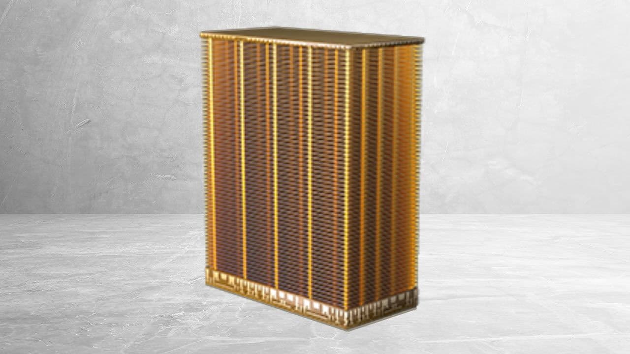
Micron has confirmed that its G11 3D NAND, set for mass production in the second half of 2027, will double bit density and lift I/O performance by 50% over its current generation. The company outlined the roadmap at a technology event this week, positioning G11 as a direct challenge to rivals in the high-stakes memory market.
How Wafer Bonding Unlocks Density Gains
At the heart of G11 is a manufacturing shift that Micron has been signaling for years. The company will bond two wafers together: one holding the 3D NAND array and another carrying the peripheral logic and I/O circuitry. This differs from Micron's long-used CMOS-under-array architecture, which places logic beneath the memory array on the same wafer.
Scott DeBoer, president and chief technology and products officer at Micron, said the timing is now right. "We had mentioned we will bring in wafer-on-wafer bonding technology at the right time when it's cost-effective, and it brings in capability that is important for the product specs at the time," he said during the event. "This G11 technology is the world's most advanced NAND."
The bonding approach allows Micron to use different process technologies for the array and the logic, potentially improving yields and performance. It also mirrors a strategy already deployed by YMTC, the Chinese memory maker that has used wafer bonding to advance its own NAND products.
Beyond G11: The Road to 400+ Layers and New Materials
G11 will feature more than 400 layers, a significant jump from the current G9 generation. Micron has not disclosed the exact layer count or the number of memory decks, but the company claims an industry-leading memory cell pitch. That suggests density gains will come from both additional layers and smaller cell dimensions.
These improvements are expected to benefit conventional high-capacity SSDs for client and data center applications, as well as emerging AI-oriented storage devices. AI workloads demand greater bandwidth and energy efficiency, and Micron's roadmap targets exactly those pain points.
Meanwhile, Micron is already developing new materials and denser memory cell architectures to extend 3D NAND scaling beyond G11. The company expects to disclose more technical details in 2027, closer to high-volume manufacturing.
Why This Matters
The memory industry is at a inflection point. AI accelerators and data-intensive workloads are straining current NAND technology, and Micron's G11 promises to ease those bottlenecks. For cloud providers and AI hardware designers, the combination of higher density, faster I/O and lower power could translate into more efficient storage tiers and lower total cost of ownership.
Competitively, Micron's move puts pressure on Samsung, Kioxia and SK Hynix to accelerate their own roadmaps. Samsung's V10 and Kioxia's BiCS10 are already in the market, but G11's claimed density and performance targets could leapfrog them. The wafer bonding approach also validates YMTC's early bet on the technology, potentially reshaping supply chain dynamics.
For end users, the impact will be felt in everything from faster consumer SSDs to more capable AI inference at the edge. As Micron ramps G11 in 2027, the memory landscape will shift toward denser, more power-efficient storage, enabling new classes of devices and services.
The Road Ahead for 3D NAND Scaling
Micron's disclosure comes as the industry grapples with the physical limits of NAND scaling. Traditional shrinking of memory cells is becoming harder and more expensive. Wafer bonding and new materials represent the next frontier, and Micron's G11 is a concrete step in that direction.
The company's plan to share more details in 2027 will be closely watched by investors and competitors alike. With mass production slated for the second half of that year, the clock is ticking for rivals to respond.


